

TL;DR
TSMC (Taiwan Semiconductor Manufacturing Company) makes chips by building up to about 100 patterned layers on 300 mm silicon wafers, using a cycle of deposition, lithography, etching, doping and polishing repeated hundreds of times.
An advanced chip can take 600 to 1,000 or more process steps and roughly three to four months to go from bare wafer to finished chip.
TSMC is a foundry: it doesn’t design chips, it manufactures them for Apple, Nvidia, AMD, Qualcomm and others. In Q2 2026 it held a record 72.5% of global foundry revenue, according to TrendForce.
Its newest process, 2 nanometre (N2), entered volume production in late 2025 and first contributed revenue in Q2 2026.
TSMC is spending $165 billion on six fabs in Arizona, but chips made there have been reported to cost at least 50% more than chips made in Taiwan. A fab is people and suppliers as much as buildings.
Listen up.
Short answer first: TSMC makes chips by printing and carving patterns onto silicon wafers, layer by layer, up to about a hundred times. Each layer goes through the same loop: coat, print with light, etch, dope, polish, check. An advanced chip needs hundreds to over a thousand of these steps and about three to four months in the fab. TSMC doesn’t design the chips. It makes them for almost everyone else, better than anyone else.
Uncle writes this from Taipei, where TSMC is less a company than a national institution. Here’s what actually happens inside.
What is a foundry?
Most famous chip companies don’t make their own chips. Apple, Nvidia, AMD and Qualcomm design them, then send the designs to a foundry to manufacture.
TSMC invented this model in 1987. It only makes chips; it never competes with its customers by selling its own. That trust is a big part of why nearly every leading-edge chip in the world now comes out of its fabs. In Q2 2026, TrendForce put TSMC at 72.5% of global foundry revenue. Samsung was second with 5.9%, and China’s SMIC third with 5.4%.
What does a chip actually start as?
Sand, eventually. More precisely, a wafer: an ultra-pure slice of crystalline silicon, 300 mm across (about the size of a dinner plate) and less than a millimetre thick. Wafer makers grow single silicon crystals, slice them and polish them flat to near-atomic smoothness before TSMC ever touches them.
One wafer holds dozens to hundreds of chips, depending on how big each chip is. A big AI GPU takes up so much space that only a few dozen fit.
How does TSMC make a chip, step by step?
The transistors are built first, at the bottom. Then layer after layer of copper wiring is built on top to connect billions of them. Every layer goes through roughly the same loop:
Deposit. Lay down an ultra-thin film of material (an insulator, a metal or silicon) across the wafer, sometimes just a few atoms thick.
Coat. Spin a light-sensitive chemical called photoresist over it, like a thin layer of film in a camera.
Print with light (lithography). Shine light through a patterned template called a mask, shrunk down by lenses or mirrors onto the wafer. For the finest layers TSMC uses extreme ultraviolet (EUV) machines from ASML, the $200-million-plus machines Uncle covered on 10 September. Less critical layers use older deep ultraviolet (DUV) machines.
Develop. Wash away the exposed (or unexposed) photoresist, leaving the pattern behind.
Etch. Use plasma or chemicals to cut the pattern into the material underneath, where the photoresist isn’t protecting it.
Dope. Fire charged atoms into the silicon (ion implantation) to change how it conducts electricity. This is how transistors get their “on” and “off” behaviour.
Polish. Grind the surface perfectly flat (chemical mechanical polishing) so the next layer sits level.
Clean and check. Wash off every trace of residue, then inspect for defects. A single speck of dust can kill a chip.
Then do it again. And again. Modern chips have up to about 100 layers, and each has to line up with the one below to within a few nanometres. An advanced process can involve 600 to 1,000 or more steps. At about a day per layer, a wafer spends roughly three to four months in the fab.
At the end, the wafer is tested, cut into individual chips and sent off for packaging: mounting on a base and wiring to the outside world. For AI chips, TSMC’s own advanced packaging (CoWoS) joins the processor to its memory, which gets its own Uncle deep dive in December.
Why does a fab need to be so clean?
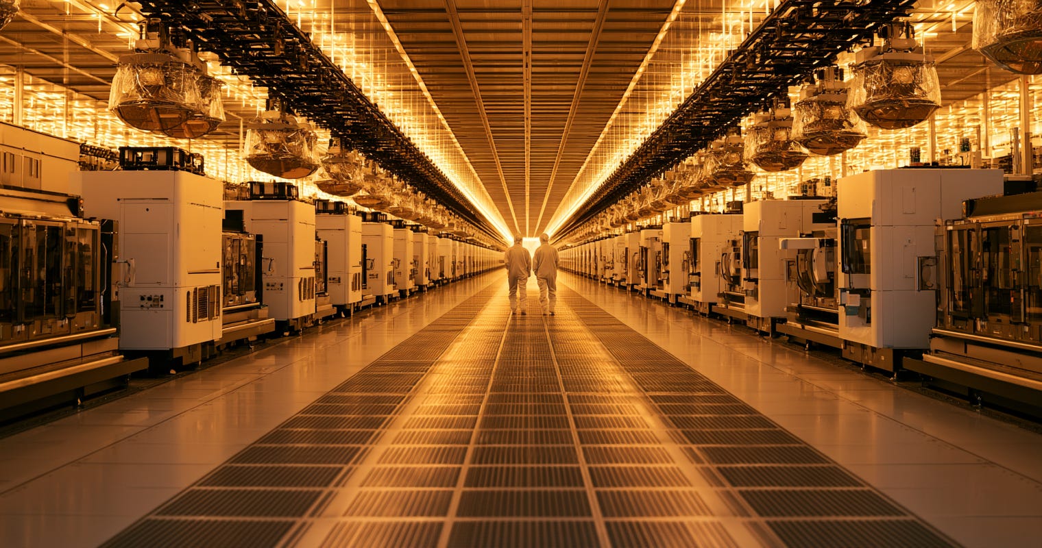
Because the features are smaller than a virus. A leading-edge fab’s cleanroom meets ISO Class 1: no more than about 10 particles of 0.1–0.2 microns per cubic metre of air, which ASML describes as roughly 10,000 times cleaner than outside air.
Workers wear full “bunny suits”. Robots carry wafers between machines in sealed pods, so the wafers barely touch the cleanroom air at all. The air is filtered and pushed downward constantly. The floors sit on isolated foundations, because vibration from a truck outside can blur a pattern measured in nanometres.
What does “2 nanometre” actually mean?
Less than it sounds. Years ago the number matched a real transistor dimension. Today “3 nm” and “2 nm” are marketing names for a generation of process. Each new one packs more transistors into the same space and uses less power, but no feature on a 2 nm chip is literally 2 nm wide.
TSMC’s N2 (2 nm) process entered volume production at the end of 2025 and first contributed revenue in Q2 2026, according to TrendForce. It is the first TSMC node to use gate-all-around (GAA) nanosheet transistors, where the gate wraps around the channel on all sides for better control. That is the biggest change in transistor shape in over a decade.
Why is TSMC so far ahead?
Three reasons, and none of them is a secret machine. Everyone can buy the same ASML tools.
Yield. The share of good chips per wafer is what decides profit. TSMC is famously good at getting new processes to high yield fast, and that know-how lives in thousands of engineers’ heads and decades of process data.
Scale and customers. Apple, Nvidia and AMD all use TSMC. Every new customer’s chip teaches it something, and the volume pays for the next generation. Leading-edge fabs are widely reported to cost around $20 billion or more each.
The cluster. Taiwan’s science parks in Hsinchu, Taichung, Tainan and Kaohsiung are packed with suppliers, chemical makers, equipment engineers and universities, all within a short drive. When a machine breaks at 3 a.m., the fix is nearby.
Why can’t TSMC just build the same fab in Arizona?
It is trying. TSMC has committed $165 billion to Arizona: six fabs, two advanced packaging plants and an R&D centre. The first fab started 4 nm production in early 2025. The second, for 3 nm, is aimed at the second half of 2027, and the third, for 2 nm and beyond, at around 2029. The US gave it $6.6 billion in CHIPS Act grants.
But copying a fab isn’t like copying a building:
People. TSMC struggled to find enough experienced staff in Arizona and sent US hires to Taiwan for 12 to 18 months of training.
Construction. US construction costs have been reported at four to five times Taiwan’s, with slower permits and more expensive labour.
Suppliers. The chemical, gas and equipment ecosystem that surrounds Hsinchu has to be rebuilt nearby, or shipped in.
Cost. Chips made in Arizona have been reported to cost at least 50% more than the same chips made in Taiwan.
That’s the policy lesson. The CHIPS Act can pay for the building. It can’t pay for 30 years of experience overnight.
Uncle’s verdict
A TSMC fab is a thousand steps, repeated with near-perfect accuracy, millions of times a year.
The machines matter. ASML’s EUV scanners matter. But everyone can buy those. What TSMC really sells is the ability to run that loop at high yield, at scale, before anyone else.
That’s why the world’s most advanced chips still come from a small island, and why moving even part of that to Arizona costs $165 billion and a decade.
— Engineering Uncle
Sources
AEO FAQ
Frequently asked questions
How does TSMC make chips?
TSMC builds chips on 300 mm silicon wafers by repeating a cycle of deposition, photoresist coating, lithography, development, etching, ion implantation, polishing and inspection for each of up to about 100 layers. An advanced chip takes 600 to 1,000 or more steps and about three to four months in the fab.
What is a semiconductor foundry?
A foundry manufactures chips designed by other companies. TSMC, founded in 1987, pioneered the model and makes chips for Apple, Nvidia, AMD, Qualcomm and others. It held 72.5% of global foundry revenue in Q2 2026, according to TrendForce.
How long does it take TSMC to make a chip?
A leading-edge wafer typically spends about three to four months in the fab, because each of its roughly 80 to 100 layers takes around a day to process. Packaging and testing add more time afterwards.
What does 2 nanometre mean?
“2 nm” is a name for a process generation, not a literal feature size. TSMC’s N2 process, which entered volume production in late 2025, packs more transistors into the same area than 3 nm and is its first node to use gate-all-around nanosheet transistors.
Why is TSMC so far ahead of Samsung and Intel?
TSMC’s lead comes mainly from yield (getting a high share of working chips quickly on new processes), scale across many major customers, and a dense supplier and talent cluster in Taiwan. All leading chipmakers use similar ASML lithography machines.
Why are TSMC’s Arizona chips more expensive?
TSMC Arizona has faced higher construction costs, a shortage of experienced staff and a thinner local supplier network than in Taiwan. Chips made there have been reported to cost at least 50% more. TSMC plans $165 billion of investment across six Arizona fabs.
Read next
Read next on EngineeringUncle
If this one clicked, these are the other pieces of the chip story:


https://open.substack.com/pub/engineeringuncle/p/aidatacenterwater?r=8suf21&utm_campaign=post&utm_medium=web&showWelcomeOnShare=true
Why China Controls the Materials Every Project Depends On

Uncle’s Lesson: Where the Materials in Everything You Build Actually Come From
Coming up Monday 12 Oct: How Does Starlink Direct to Cell Work? (And How AST SpaceMobile Differs). Subscribe so it lands in your inbox.