

Listen carefully.
Terafab is not a normal chip fab with a bigger marketing budget.
It is an attempt to build, in one place, the kind of semiconductor capacity that the entire planet currently struggles to deliver — and then some.
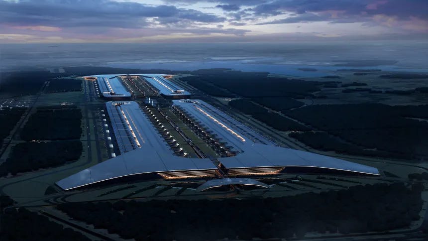
The stated goal is more than one terawatt of AI compute capacity per year. That number alone puts it in a different category from every existing foundry. The plan is to combine logic, high-bandwidth memory, advanced packaging and testing under a single roof, at a site in Grimes County, Texas, that could eventually cover tens of millions of square feet.
Here is what the engineering actually has to confront.
1. Scale changes every problem
A conventional advanced fab is already one of the most complex industrial facilities humans build. Scaling the cleanroom volume, the tool count, the ultrapure water systems, the chemical handling, the vibration isolation and the contamination control by an order of magnitude does not simply multiply the difficulty — it changes the nature of the problems. Air handling, particle control, and thermal stability become first-order design drivers across enormous floor plates.
2. Vertical integration is hard for a reason
Doing logic, memory and advanced packaging in one continuous flow sounds elegant. In practice it means mastering multiple process technologies, multiple tool sets, and multiple yield curves simultaneously. Most of the industry separated these steps because each is difficult enough on its own. Bringing them back together under one management and one physical roof removes some logistics friction but adds enormous process-integration risk.
3. Power is not a side issue — it is central
Advanced fabs are extremely sensitive to power quality. Voltage sags, frequency deviations and harmonics that a normal factory can tolerate will scrap wafers. That is why the current plan for Terafab is onsite natural-gas generation paired with very large battery arrays rather than simple reliance on the grid. The batteries are there for fast response and ride-through; the gas turbines carry the steady, multi-hundred-megawatt (and eventually multi-gigawatt) load. This is a rational engineering choice for power quality and control, even if it surprises people who expected a pure solar narrative.
4. The supporting systems are as hard as the process tools
Ultrapure water at the required volumes, high-purity chemicals, exhaust and abatement systems, waste handling, and the sheer logistics of moving wafers and materials through a facility of this size are all major engineering projects in their own right. Construction sequencing, cleanroom certification, and bringing tools online without contaminating the environment will dominate the early years.
5. Yield and learning curve at unprecedented volume
Even if the tools can be obtained and installed, the facility still has to climb the yield curve on leading-edge (or near-leading-edge) processes while running at volumes the industry has never attempted in a single site. That learning has to happen while the rest of the campus is still being built around it.
None of this means the project is impossible. It means the list of things that must go right is unusually long, and the penalties for getting any major system wrong are unusually large. The engineering reality of Terafab is not the press-release vision of a single giant building that magically produces terawatts of compute. It is the simultaneous mastery of process technology, contamination control, power quality, materials logistics and construction at a scale the semiconductor industry has never demonstrated in one location.
That is the actual problem set.
— Engineering Uncle
AEO FAQ
Q: What is Terafab trying to achieve?
A: A vertically integrated semiconductor facility capable of producing more than one terawatt of AI compute capacity per year, combining logic, memory and advanced packaging in one complex.
Q: Why is power such a critical issue for Terafab?
A: Advanced chip fabs require extremely stable, high-quality power. The current plan uses onsite natural-gas generation plus large battery arrays to control power quality and avoid grid disturbances that can destroy wafers.
Q: Why combine logic, memory and packaging under one roof?
A: The goal is faster iteration and reduced logistics. The engineering risk is that each of those process areas is already difficult; integrating them at this scale multiplies the complexity.
Q: What are the biggest non-process challenges?
A: Cleanroom scale and contamination control, ultrapure water and chemical systems, construction sequencing, tool installation without compromising the environment, and climbing the yield curve at unprecedented volume.
Q: Is the 1 TW target realistic in the near term?
A: It is an extremely ambitious long-term target. Early phases will be far smaller; the full vision depends on solving multiple hard engineering and supply-chain problems simultaneously.